Gas to Solid: Deposition Science & Coating
Deposition science investigates the transformation of a substance from gas to solid, a process critical in advanced material engineering. Chemical Vapor Deposition (CVD), a widely used technique, facilitates gas to solid conversion on substrates to form thin films. Researchers at institutions like the Massachusetts Institute of Technology (MIT) explore novel coating applications derived from gas to solid methods for enhanced durability. The quartz crystal microbalance (QCM) serves as an essential instrument for monitoring gas to solid phase changes at the microscale, providing precise measurements of deposition rates and material properties.
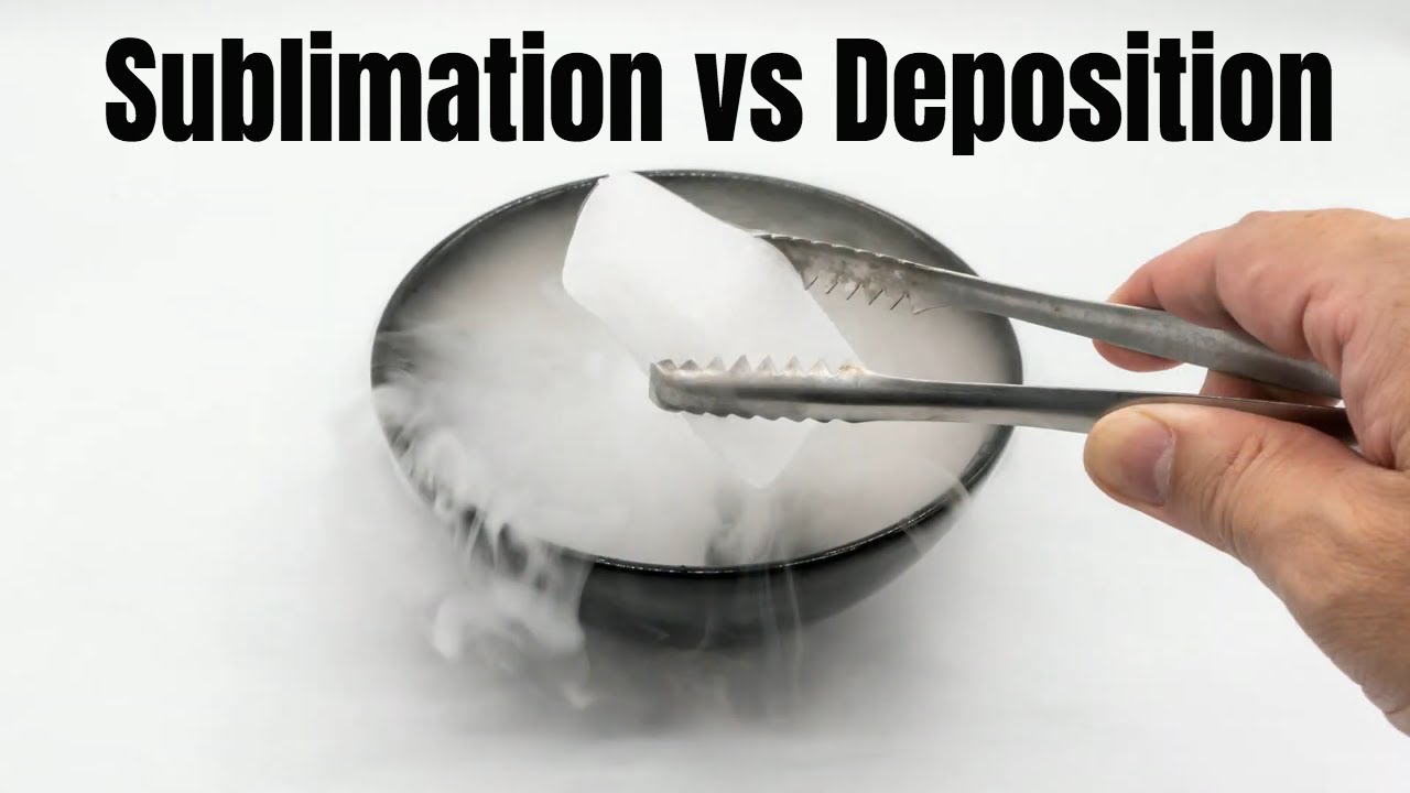
Image taken from the YouTube channel MooMooMath and Science , from the video titled Sublimation vs Deposition .
Unveiling the World of Gas-to-Solid Deposition
Gas-to-solid deposition represents a suite of sophisticated processes wherein gaseous precursors, meticulously selected and prepared, are transformed into solid materials.
This transformation hinges on controlled chemical reactions or physical processes that occur either within a reaction chamber or directly onto a substrate. The result is the formation of thin films and coatings, materials of paramount importance across a spectrum of industries.
The Significance of Thin Films and Coatings
Thin films and coatings, products of gas-to-solid deposition, are not merely surface treatments. They are integral components that impart enhanced functionalities and protection to a diverse range of products.
The significance of these films lies in their ability to tailor material properties without altering the bulk characteristics of the underlying substrate. This capability allows for unprecedented control over surface properties such as hardness, corrosion resistance, optical characteristics, and electrical conductivity.
Applications Across Industries
The versatility of gas-to-solid deposition has led to its widespread adoption across numerous sectors:
-
Electronics: Microelectronics relies heavily on thin films for fabricating semiconductors, integrated circuits, and display technologies. The precision offered by techniques like Atomic Layer Deposition (ALD) is critical for creating the intricate structures found in modern electronic devices.
-
Aerospace: In the aerospace industry, coatings derived from gas-to-solid deposition enhance the performance and lifespan of critical components. These coatings provide thermal protection, wear resistance, and corrosion protection in harsh operating environments.
-
Automotive: The automotive sector utilizes coatings to improve fuel efficiency, reduce emissions, and enhance the aesthetic appeal and durability of vehicles. Applications range from wear-resistant engine components to decorative coatings on exterior surfaces.
Fundamental Principles: A Brief Overview
At its core, gas-to-solid deposition involves a series of fundamental processes that dictate the quality and characteristics of the resulting film. These processes include:
-
Adsorption: The adhesion of gas molecules to the substrate surface.
-
Surface Diffusion: The movement of adsorbed atoms or molecules across the substrate surface.
-
Nucleation: The formation of stable nuclei, serving as the foundation for film growth.
-
Chemical Reaction (in CVD): The chemical transformation of gas precursors.
-
Desorption: The release of molecules from the substrate surface.
Understanding these principles is essential for controlling film properties such as thickness, composition, and morphology.
Fundamental Processes: The Building Blocks of Film Formation
The transformation of gaseous precursors into functional solid films is a complex orchestration of fundamental processes. Understanding these processes is critical to controlling film properties such as composition, morphology, and ultimately, performance. These fundamental processes, including nucleation, adsorption/desorption, and surface chemistry, define how the building blocks of the material assemble and grow into a coherent film. This section will delve into the intricacies of these processes.
Nucleation: Seeding Solid Formation
Nucleation marks the inception of solid-phase formation from the gaseous phase. It is the genesis of thin film growth. The process begins with the stochastic aggregation of adatoms (adsorbed atoms) on the substrate surface.
These adatoms must overcome an energy barrier to form stable nuclei. Once a stable nucleus forms, it acts as a seed for further growth, drawing more adatoms from the surrounding environment.
The rate of nucleation is heavily influenced by factors such as substrate temperature, supersaturation of the gaseous precursor, and the presence of nucleation sites or defects on the substrate surface. High nucleation density results in finer-grained films, while lower density leads to larger crystalline domains.
Adsorption and Desorption: The Dynamic Duo of Surface Coverage
Adsorption and desorption are the yin and yang of gas-surface interactions. Adsorption is the process where gas molecules or atoms adhere to the substrate surface. This adhesion is driven by either physical forces (physisorption) or chemical bonding (chemisorption).
Physisorption involves weak van der Waals forces and is typically reversible. Chemisorption, on the other hand, involves the formation of chemical bonds and is often irreversible at lower temperatures. The strength of the adsorption dictates the residence time of the adatoms on the surface.
Desorption is the opposing process. It is when adsorbed species leave the surface and return to the gaseous phase. This process is thermally activated; adatoms must gain enough energy to overcome the binding energy holding them to the substrate.
The balance between adsorption and desorption determines the surface coverage of the precursor species. Higher substrate temperatures tend to favor desorption, reducing the surface concentration of adatoms available for film growth.
Surface Chemistry: Reactions at the Interface
Surface chemistry encompasses the chemical reactions that occur on the substrate surface. These reactions are critical for transforming the adsorbed precursor species into the desired solid material.
The nature of these reactions depends heavily on the specific precursors used, the substrate material, and the process conditions. Catalytic effects from the substrate can also play a significant role in the reaction kinetics.
For instance, in CVD, gaseous precursors decompose on the heated substrate surface, releasing volatile byproducts and leaving behind the desired film material. The efficiency and selectivity of these reactions determine the film's composition, purity, and microstructure.
Thin Film Growth Kinetics: Modeling the Deposition Process
Thin film growth kinetics refers to the study of the rates and mechanisms by which thin films are formed. Understanding these kinetics is crucial for controlling film thickness, uniformity, and microstructure.
Several models have been developed to describe thin film growth, including the Volmer-Weber (island growth), Frank-van der Merwe (layer-by-layer growth), and Stranski-Krastanov (layer-plus-island growth) modes. The growth mode is determined by the surface energies of the substrate, film, and interface.
Factors such as deposition temperature, precursor flux, and substrate bias can dramatically affect growth kinetics. By carefully controlling these parameters, the film’s properties can be tailored for specific applications.
Deposition Techniques: CVD and PVD Methods Explored
The ability to manipulate materials at the atomic level is a cornerstone of modern technology. Among the various techniques used to create thin films and coatings, Chemical Vapor Deposition (CVD) and Physical Vapor Deposition (PVD) stand out as the most prominent.
Each method leverages distinct physical and chemical principles to transform source materials into solid films. Understanding the nuances of CVD and PVD is crucial for tailoring material properties and optimizing performance in diverse applications.
Chemical Vapor Deposition (CVD)
Chemical Vapor Deposition (CVD) relies on chemical reactions to deposit thin films. Gaseous precursors are introduced into a reaction chamber where they decompose or react on a heated substrate. This process results in the formation of a solid film on the substrate surface.
CVD Precursors
The choice of precursor is critical in CVD. Precursors must be volatile, stable at room temperature, and capable of undergoing controlled decomposition at elevated temperatures.
Common examples include:
-
Metal halides: Tungsten hexafluoride (WF6) for tungsten films.
-
Organometallic compounds: Trimethylgallium (TMGa) for gallium-containing films.
-
Silanes: Silane (SiH4) for silicon films.
The purity and reactivity of these precursors directly impact the quality and composition of the deposited film.
CVD Reactors
CVD reactors are designed to provide a controlled environment for the chemical reactions to occur. Different reactor configurations exist, each with its advantages and disadvantages.
-
Hot-wall reactors: The entire reactor is heated, providing uniform temperature distribution.
-
Cold-wall reactors: Only the substrate is heated, reducing gas-phase reactions.
-
Vertical and horizontal reactors: Differ in the orientation of the substrate and gas flow.
The selection of reactor type depends on the specific requirements of the deposition process.
CVD Variants
Several variants of CVD have been developed to enhance film properties and deposition rates.
Plasma-Enhanced CVD (PECVD)
PECVD utilizes plasma to enhance the decomposition of precursors at lower temperatures. This is particularly useful for depositing films on temperature-sensitive substrates.
The plasma generates reactive species that facilitate chemical reactions, leading to higher deposition rates and improved film quality.
Atomic Layer Deposition (ALD)
ALD is a self-limiting process that deposits films one atomic layer at a time. It involves sequential exposure of the substrate to different precursors, each reacting only with the surface.
This precise control over film thickness and composition makes ALD ideal for applications requiring ultra-thin and highly conformal films.
Physical Vapor Deposition (PVD)
Physical Vapor Deposition (PVD) techniques involve the physical transfer of material from a source to a substrate. Unlike CVD, PVD does not rely on chemical reactions. Instead, it uses processes such as evaporation or sputtering to create a vapor of the source material, which then condenses onto the substrate.
Sputtering
Sputtering involves bombarding a target material with energetic ions, typically argon ions. The impact of these ions causes atoms from the target to be ejected and deposited onto the substrate.
Sputtering is a versatile technique that can be used to deposit a wide range of materials, including metals, ceramics, and compounds.
Evaporation
Evaporation involves heating a source material in a vacuum until it evaporates. The vaporized material then travels to the substrate, where it condenses to form a thin film.
Evaporation is commonly used to deposit metals and simple compounds.
PVD Systems
PVD systems are designed to create and control the deposition environment.
-
Vacuum chambers: Maintain a low-pressure environment to minimize contamination and facilitate the transport of vaporized material.
-
Sputtering targets: Serve as the source material in sputtering processes.
-
Evaporation sources: Provide the energy needed to vaporize the source material in evaporation processes.
The design and operation of PVD systems are critical for achieving high-quality films with desired properties.
Materials and Their Properties: From Silicon to Diamond-Like Carbon
Having explored the fundamental deposition techniques, we now turn our attention to the materials themselves. The selection of a material is paramount, dictating the functionality and performance of the final coating. From the ubiquitous silicon to advanced materials like diamond-like carbon, understanding their properties is crucial for tailoring applications.
Common Materials in Gas-to-Solid Deposition
The world of thin films and coatings boasts a diverse array of materials, each offering unique advantages. We will examine three prominent examples: silicon, titanium nitride, and diamond-like carbon, highlighting their distinct characteristics and applications.
Silicon (Si): The Cornerstone of Microelectronics
Silicon, a semiconductor par excellence, reigns supreme in the realm of microelectronics. Its ability to be precisely doped, combined with its natural oxide formation, has made it the backbone of transistors and integrated circuits.
In thin film form, silicon finds applications in solar cells, thin-film transistors (TFTs) for displays, and various sensor technologies. The precise control over its deposition, doping, and structural properties allows for the creation of complex electronic devices.
Titanium Nitride (TiN): Hardness and Wear Resistance
Titanium Nitride (TiN) stands out as a hard, wear-resistant coating, renowned for its golden color. Its exceptional hardness makes it ideal for cutting tools, extending their lifespan and improving machining efficiency.
Beyond cutting tools, TiN coatings are employed in medical implants, decorative finishes, and as a diffusion barrier in microelectronics. Its chemical inertness and biocompatibility further broaden its applicability.
Diamond-Like Carbon (DLC): Low Friction and Protection
Diamond-Like Carbon (DLC) represents a class of amorphous carbon materials characterized by a high percentage of sp3-bonded carbon atoms. This bonding endows DLC with exceptional hardness, chemical inertness, and, most notably, low friction.
DLC coatings find extensive use in automotive components, such as engine parts and bearings, reducing friction and improving fuel efficiency. They are also employed in medical devices and hard drives due to their biocompatibility and protective properties.
Impact of Deposition Parameters on Film Morphology
The properties of a deposited film are not solely determined by the material itself, but also by the deposition parameters employed. These parameters, including temperature, pressure, gas flow rates, and substrate bias, exert a profound influence on the film's morphology.
Morphology encompasses the surface structure, grain size, density, and overall texture of the film.
The Role of Temperature
Substrate temperature during deposition dramatically affects adatom mobility. Higher temperatures promote surface diffusion, leading to larger grain sizes and smoother films. Conversely, lower temperatures result in smaller grain sizes and rougher surfaces.
Pressure and Gas Flow
Chamber pressure and gas flow rates influence the mean free path of the depositing species. This, in turn, affects the uniformity and conformality of the film. Higher pressures can lead to increased scattering and non-uniform deposition.
Substrate Bias
Substrate bias (applying a voltage to the substrate) can influence the energy of the incoming ions, altering the film density and stress. Applying a negative bias can lead to ion bombardment, resulting in denser films with compressive stress.
In conclusion, the careful selection of materials and the precise control over deposition parameters are essential for engineering thin films and coatings with tailored properties. This allows for the creation of materials with specific functionalities, driving innovation across numerous industries.
Key Components and Technologies: The Machinery Behind the Magic
Having explored the fundamental deposition techniques, we now turn our attention to the materials themselves. The selection of a material is paramount, dictating the functionality and performance of the final coating. From the ubiquitous silicon to advanced materials like diamond-like carbon, a diverse palette of options exists. However, the deposition process itself hinges on a complex interplay of specialized components and technologies. These act as the unsung heroes, orchestrating the transformation of gaseous precursors into functional solid films.
The Foundation: Substrates
The substrate serves as the very foundation upon which the thin film is grown. Its properties, including surface roughness, temperature stability, and chemical compatibility, exert a profound influence on the resulting film's characteristics. The choice of substrate is dictated by the intended application and the deposition process itself. It is important to consider these substrate factors to maintain final thin film quality.
For instance, a silicon wafer might be favored for microelectronic applications due to its crystalline structure and thermal conductivity. Conversely, a polymer film could be employed for flexible electronics, emphasizing conformability over high-temperature resistance.
The Controlled Environment: Vacuum Technology
A pristine and carefully controlled environment is indispensable for high-quality thin film deposition. Vacuum technology plays a pivotal role in achieving this, enabling the precise manipulation of pressure, temperature, and gas composition within the deposition chamber.
By evacuating the chamber to extremely low pressures, the mean free path of gas molecules is significantly increased, minimizing unwanted collisions and reactions. This ensures that the precursor gases reach the substrate surface unimpeded, promoting uniform and controlled film growth.
Furthermore, vacuum technology mitigates contamination by removing residual gases and impurities that could otherwise compromise the film's purity and properties.
The Alchemist's Chamber: CVD Reactors and PVD Systems
The reactor, in the context of Chemical Vapor Deposition (CVD), serves as the alchemist's chamber, where gaseous precursors undergo controlled chemical reactions to form the desired solid film. Different reactor designs exist, each tailored to specific process parameters and material requirements.
Hot-wall reactors, for instance, utilize external heating to maintain a uniform temperature throughout the chamber, promoting homogeneous deposition. Cold-wall reactors, on the other hand, selectively heat the substrate, minimizing gas-phase reactions and enhancing film quality.
In Physical Vapor Deposition (PVD), the PVD system takes center stage, employing physical processes such as sputtering or evaporation to generate a flux of atoms or molecules that deposit onto the substrate. These systems often incorporate sophisticated control mechanisms to regulate the deposition rate, film thickness, and composition.
The Crucible of Creation: Vacuum Chambers, Sputtering Targets, and Evaporation Sources
At the heart of most deposition systems lies the vacuum chamber, a sealed enclosure that provides a controlled atmosphere for the deposition process. Its design must be robust and leak-tight, capable of withstanding extreme pressures and temperatures.
Within the chamber, specialized components facilitate the generation and transport of the deposition material.
Sputtering targets serve as the source material in sputtering processes, bombarded by energetic ions that eject atoms from the target surface.
Evaporation sources, conversely, heat the source material to its vaporization point, creating a vapor flux that deposits onto the substrate. The choice of source depends on the material's properties and the desired deposition rate.
The Spark of Innovation: Plasma Generators
In Plasma-Enhanced CVD (PECVD), a plasma generator is employed to create a reactive plasma within the deposition chamber. This plasma consists of ionized gases and energetic electrons, which promote chemical reactions at lower substrate temperatures compared to conventional CVD.
This feature is particularly advantageous for depositing films onto temperature-sensitive substrates, such as polymers. The plasma also enhances the deposition rate and film density.
The Metronome of Deposition: Quartz Crystal Microbalance (QCM)
Accurate measurement and control of the deposition rate are crucial for achieving films with desired thickness and properties. The Quartz Crystal Microbalance (QCM) offers a highly sensitive method for real-time monitoring of deposition processes.
QCM utilizes a quartz crystal oscillator whose resonant frequency changes proportionally to the mass deposited on its surface. By precisely measuring this frequency shift, the deposition rate and film thickness can be determined with remarkable accuracy. This allows for fine-tuning of the deposition parameters and ensures reproducibility of the process.
Characterization Techniques: Analyzing Film Properties
Having explored the fundamental deposition techniques, we now turn our attention to the materials themselves. The selection of a material is paramount, dictating the functionality and performance of the final coating. From the ubiquitous silicon to advanced materials like diamond-like carbon, understanding and tailoring the properties of these films is crucial. This requires a suite of sophisticated characterization techniques, each providing unique insights into the film's structure, morphology, and composition.
Unveiling Film Secrets: The Importance of Characterization
The deposition process, while carefully controlled, can still yield films with variations in thickness, density, and crystalline structure. These variations directly impact the film's performance. Therefore, post-deposition characterization is essential. It ensures the film meets the required specifications. It also provides feedback for optimizing the deposition process itself.
X-Ray Diffraction (XRD): Decoding Crystalline Structure
X-Ray Diffraction (XRD) stands as a cornerstone technique for probing the crystalline structure of deposited materials. By directing a beam of X-rays onto the sample and analyzing the diffraction patterns, XRD reveals invaluable information about the material's phase composition, crystallite size, and preferred orientation.
Specifically, the angles at which the X-rays are diffracted correspond to the spacing between atomic planes in the crystal lattice, according to Bragg's Law. Analyzing the position and intensity of the diffraction peaks allows us to identify the crystalline phases present, determine the lattice parameters, and quantify the degree of crystallinity.
Applications of XRD in Film Analysis
XRD is particularly useful for:
- Phase Identification: Identifying the different crystalline phases present in the film.
- Crystallite Size Determination: Estimating the average size of the crystalline domains.
- Texture Analysis: Determining if the film exhibits a preferred crystallographic orientation.
- Strain Measurement: Assessing the residual stress within the film.
Scanning Electron Microscopy (SEM): Visualizing Surface Morphology
Scanning Electron Microscopy (SEM) provides high-resolution images of the film's surface morphology. A focused beam of electrons scans the sample, and the emitted secondary electrons are collected to create an image. This allows for detailed visualization of surface features such as grain size, surface roughness, and the presence of defects.
Advantages of SEM
- High Magnification: Capable of imaging at magnifications up to hundreds of thousands of times.
- High Resolution: Provides detailed images of surface features at the nanometer scale.
- Versatile Applications: Can be used to image a wide range of materials, including metals, semiconductors, and polymers.
Interpreting SEM Images
Analyzing SEM images allows researchers to:
- Determine the grain size and shape of the film.
- Identify surface defects, such as cracks or pinholes.
- Assess the uniformity and conformity of the film.
Atomic Force Microscopy (AFM): Probing Surface Topography and Roughness
Atomic Force Microscopy (AFM) goes beyond imaging, offering a means to measure surface topography and roughness at the atomic level. A sharp tip, mounted on a cantilever, scans the surface. Interactions between the tip and the sample surface are used to create a three-dimensional map of the topography.
AFM Modes of Operation
AFM can be operated in various modes, including:
- Contact Mode: The tip is in continuous contact with the surface.
- Tapping Mode: The tip oscillates near its resonant frequency and intermittently taps the surface.
- Non-Contact Mode: The tip oscillates above the surface without making contact.
AFM Measurements
AFM allows for the quantification of key surface parameters:
- Surface Roughness: Measured as the root mean square (RMS) roughness or average roughness.
- Feature Size: Determining the size and distribution of surface features.
- Adhesion Forces: Measuring the forces between the tip and the sample surface.
Ellipsometry: Measuring Thickness and Optical Properties
Ellipsometry is a powerful optical technique for characterizing thin film thickness and optical properties. It measures the change in polarization of light upon reflection from the sample surface. By analyzing these changes, ellipsometry can determine the film's thickness, refractive index, and extinction coefficient.
The Principles of Ellipsometry
Ellipsometry measures two parameters:
- Ψ (Psi): The amplitude ratio of the p- and s-polarized light.
- Δ (Delta): The phase difference between the p- and s-polarized light.
These parameters are related to the optical constants and thickness of the film.
Advantages of Ellipsometry
- Non-Destructive: Does not damage the sample.
- High Sensitivity: Can measure films as thin as a few angstroms.
- Versatile: Can be used to characterize a wide range of materials.
Interpreting Ellipsometry Data
The measured ellipsometric parameters are fitted to a mathematical model to extract the film's thickness and optical constants. The accuracy of the results depends on the quality of the model and the accuracy of the measurements.
Applications of Gas-to-Solid Deposited Coatings: Real-World Impact
Having explored the characterization techniques crucial to verifying film properties, we now turn our attention to the real-world impact of gas-to-solid deposited coatings. Their versatility has led to widespread adoption across numerous industries, improving product performance, extending lifespans, and enabling novel functionalities. This section delves into specific applications, highlighting the tangible benefits derived from these advanced materials.
Enhancing Durability: Wear-Resistant Coatings
One of the most significant applications of gas-to-solid deposition lies in creating wear-resistant coatings. These coatings are engineered to withstand harsh conditions, protecting underlying materials from abrasion, erosion, and corrosion. Their impact is most evident in tribology and the manufacturing of cutting tools.
Tribological Applications
Tribology, the study of friction, wear, and lubrication, heavily relies on specialized coatings to minimize energy loss and component degradation. In automotive engineering, for instance, coatings deposited on engine components such as piston rings and cylinder liners dramatically reduce friction, enhancing fuel efficiency and prolonging engine life.
Diamond-like carbon (DLC) coatings, known for their exceptional hardness and low coefficient of friction, are often employed in these applications. These DLC coatings provide a robust barrier against wear, ensuring the reliable operation of critical components under demanding conditions.
Cutting Tool Technology
The performance of cutting tools, such as drill bits and milling cutters, is fundamentally linked to the properties of their surface coatings. Coatings like titanium nitride (TiN), titanium aluminum nitride (TiAlN), and chromium nitride (CrN) are routinely applied via PVD techniques to enhance hardness, thermal stability, and oxidation resistance.
These coatings enable cutting tools to operate at higher speeds and temperatures, leading to increased productivity and improved surface finish of machined parts. The use of advanced coatings has revolutionized the machining industry, enabling the efficient processing of even the most challenging materials.
Surface Protection and Beyond
Beyond wear resistance, gas-to-solid deposited coatings offer diverse functionalities, including corrosion protection, thermal barriers, and optical modifications. The breadth of these applications underscores the transformative potential of this technology.
Video: Gas to Solid: Deposition Science & Coating

FAQs: Gas to Solid Deposition Science & Coating
What is deposition in the context of materials science?
Deposition is the process where a thin film or coating is created by transforming a material from one state to another. In "gas to solid" deposition, the material starts as a gas or vapor and is converted into a solid film on a substrate.
How does gas to solid deposition create coatings?
Gas to solid deposition techniques involve introducing a gaseous precursor containing the desired coating material into a chamber. Chemical reactions or physical processes then cause the gas to condense or react, forming a solid layer on a surface.
What are some common applications of gas to solid coatings?
These coatings are used in a wide range of industries. Examples include microelectronics (semiconductors), optical coatings for lenses, protective coatings for tools, and thin films in solar cells. The gas to solid transition allows for precise control over film thickness and composition.
What are the advantages of using a gas as the initial phase for coating?
Using a gas allows for excellent conformality. Gases can easily access complex geometries and coat surfaces evenly. Additionally, "gas to solid" methods often permit precise control over the deposition rate and film properties, leading to high-quality coatings.
So, that's the gist of gas to solid deposition! Pretty cool, right? It’s amazing how transforming a gas directly into a solid coating opens up a world of possibilities for improving and protecting all sorts of materials. Who knew turning something into nothing and back again could be so useful?